晶圆回收市场势头良好 2010年将达8.59亿美元
来源:大半导体产业网发布时间:2008-05-0114浏览
询问 AI
SEMI市场研究报告显示,2007年回收晶圆市场预计为6.79亿美元,2010年将达到8.59亿美元。市场增长由每平方英寸销售价格较高的300mm晶圆带动。然而,由于供应商激增,市场将承受巨大的价格压力,尤其是300mm晶圆。200mm及以下晶圆预计保持相对稳定,原因是供应收紧以及生产线较高的利用率。目前日本、台湾和北美是全球最大的三个晶圆回收市场。欲获更多信息,请访问:
http://wps2a.semi.org/wps/portal/_pagr/135/_pa.135/745/highlights?&dFormat=application/msword&docName=P043626
The Silicon Reclaim Wafer Market is expected to grow 27% by 2010.
By Lara Chamness, senior market analyst
SEMI Industry Research and Statistics
The worldwide reclaim wafer market is estimated at $679 million in 2007 and forecasted to reach $859 million in 2010. Growth is driven by 300 mm, which maintains higher average selling prices on a square inch basis. However, due to the proliferation of suppliers, intense price pressure will continue, specifically on 300 mm. Pricing of 200 mm and smaller wafers is expected to remain relatively stable due to the tight silicon supply situation and high utilization rates of these lines.
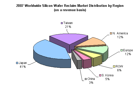
The Japan region is the largest reclaim market in terms of both revenue and numbers of wafers and it is expected to remain so for the duration of this forecast because of the prominent position of the reclaim companies there. Taiwan is the second largest market region for the reclaim market, followed by North America.
Due to the high cost of prime silicon wafers, semiconductor manufacturers run more affordable test and/or “dummy” wafers through their fab lines to optimize and monitor their manufacturing processes. Some of these wafers are made from reclaimed silicon wafers which, while not suitable for fabricating devices, are suitable for metrology and testing. When silicon wafers have been used for testing purposes or when prime silicon wafers are abandoned because of flaws in the design or manufacturing process, the device manufacturer can either send these wafers to a reclamation facility to remove processed films and materials from the wafer or do the reclaim in-house. Removal of films and materials is achieved through the application of chemicals. Reclaimed silicon wafers are then ground and polished and returned to the fab, with the cycle repeating until the reclaimed wafer is no longer useable.
Cycle time and logistics support continue to be important aspects of the reclaim wafer market. Many smaller regional suppliers exist simply because of these factors. Increasing fuel and energy costs appear to benefit these smaller suppliers in that it is not economical to transport non-device wafers to be cleaned to an out-of-town reclamation facility.
Over the past few years, concern around silicon supply has increased as the solar industry’s demand for silicon outstrips capacity. This has increased silicon pricing, including scrap silicon, significantly. At the same time, average selling prices of smaller diameter reclaim wafers has stabilized after declining for several years. This stabilization of price has been attributed to: high-utilization of lines running smaller wafer sizes, “bottoming out” of selling prices, and the tight supply for new test and monitor wafers due to the surging demand for silicon from the solar market.
A recently SEMI published report, Silicon Reclaim Wafer Characterization Summary, provides details on the 2007 silicon wafer reclaim for the semiconductor market and provides a forecast to 2010. Seven regions of the world are covered in this report including North America, Japan, Europe, Korea, Taiwan, China, and Rest of World (ROW). Market estimates for reclaim wafers include semiconductor applications including equipment and IC manufacturing markets.
Please click here for additional information about this new report as well as a list of tables and figures.
新闻来源:大半导体产业网,文中所述为作者独立观点,不代表icspec立场。更多精彩资讯请下载icspec App。如对本稿件有异议,请联系微信客服specltkj。