
博文速递:Integrated Clock and Power Gating
来源:IP与SoC设计发布时间:2024-07-082911浏览
询问 AIIntegrated Clock and Power Gating
Clock Gating and Power Gating are two most commonly used design methods to save dynamic and leakage power respectively. How about integrating the two solutions such that they complement each other? In this post, I will talk about a simple way to do so.
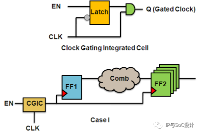
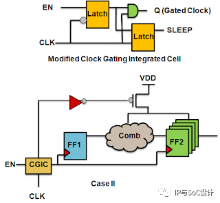
Clock Gating is accomplished by using Clock Gating Integrated Cell (CGIC) which gates the clock to the sequential elements present in its fan-out when the enable signal is logic 0. Power Gating structures may be of two types: Simple Power Gating and State Retention Power Gating. Using the former technique, the output of the logic gates slowly leaks the charge at the output and thereby when the SLEEP signal is de-asserted, one cannot predict the logic value at the output. The latter technique is able to retain the state at the output which was last present before asserting the SLEEP signal.
Let's take up a few plausible scenarios:
•Case I - Normal Case: Which employs only conventional clock gating. It is depicted in the figure.
•Case II - When one does not need to retain the states of the combinatorial cells or the sequential elements. One possible scenario could be in the case of a standalone IP, which is not comunicating with any other IP on the SoC. Here one can use thee simple power gating where the SLEEP signal is derived from the CGIC itself using a latch, as depicted in the figure below. Doing so, we would save both dynamic and leakage powers.
•Case IIII - When one does not need to retain the states of the combinatorial cells, but the sequential outputs need to be safe-stated. Possible use-case could be where only the sequential outputs communicate with other IPs on the SoC. This can be accomplished by using State Retention Flip Flops instead of the conventional flip-flops.
•Case IV - When both the combinatorial cells and the sequential cells interact with other IPs. But the previous value need not be required. Since it is a classic case of interaction between "switchable power domain" with" always ON", it entails the use of isolation cells between such power domain crossings. It must be noted that in such a case, isolation cell would always be present in the always ON power domain, i.e., it would receive it's VDD supply from the always ON power domain supply. This is because, when the switchable power domain in OFF, the isolation cell can function only if receives the power supply!
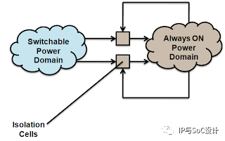
Isolation Cells can be simple cells like AND or an OR gate, which receive one input in a way that, irrespective of the second input coming from the switchable power domain, the value would be controllable. For example, logic 0 for AND gate and logic 1 for an OR gate. I will try to take this up in a separate post.
If any content of this article infringes, please contact us to remove this article.
本文内容仅代表作者观点,不代表平台观点。
如有任何异议,欢迎联系我们。
如有侵权,请联系删除。

新闻来源:IP与SoC设计,文中所述为作者独立观点,不代表icspec立场。更多精彩资讯请下载icspec App。如对本稿件有异议,请联系微信客服specltkj。